July August 2024 issue of Chip Scale Review
Over the past decade there has been a st rong push for improved electronics performance by using smaller designs; this in turn, has st imulated rapid advances in integrated technologies. Among these, 3D integration methods stand out as particularly promising. They unlock remarkable potential in terms of performance, size, efficiency, and functionality. Indeed , by vertically stacking multiple layers, 3D integration facilitates the combination of multiple functions within a tight space, enhancing performance while limit ing power consumpt ion. As a result, 3D stacked memories, chiplets, and heterogeneous integration are all gaining traction. Nevertheless, in recent years, complementary metaloxide semiconductor (CMOS) imager sensors (CIS) have clearly led the way in 3D integration. Among the emerging technologies in image sensing, a key trend is 3D multi-layer stacking. Al ready, 2-layer based imagers benefit from 3D hybrid-bonded stacking methods that make it possible to combine two separately-optimized technologies: dedicated pixel tech nolog y ( low noise, high dynamics, high QE), and advanced analog and digital CMOS (high-density, low-power). To further advance this multi-layer integration, a third layer can be added. Three-layer integration is particularly interesting because, in addition to allowing separate optimization of the individual layers, it offers additional silicon to implement new functions, place innovative partitioning solutions, or use different advanced technology nodes. Three-layer approaches thereby contribute to the pursuit of the pixel shrink race , while maintaining optical performances. They also make it possible to envisage the direct implementation of a neural network and memory, to build artificial intelligence (AI) into the sensor itself. The technologies required for this new generat ion of smart imagers based on embedded AI a re being developed by CEA-Let i within the framework of the IRT Nanoelec/Smart Imager Program that involves CEA, STMicroelectronics, Siemens EDA, Prophesee, Lynred, and Grenoble INPUGA [1]. The program tackles all the key challenges, from innovative architectures to the design and development of silicon technologies. In particular, the combination of hybrid bonding and high-density through-silicon vias (HD TSVs) is promising for the integration of the various components of imagers. This ar ticle presents CEA-Leti’s silicon technology developments involving wafer-to-wafer hybrid bonding and HD TSVs, with recent key demonstrations of 2-layer and 3-layer integrations. These demonstrations pave the way to the next generation of smart imagers (Figure 1).
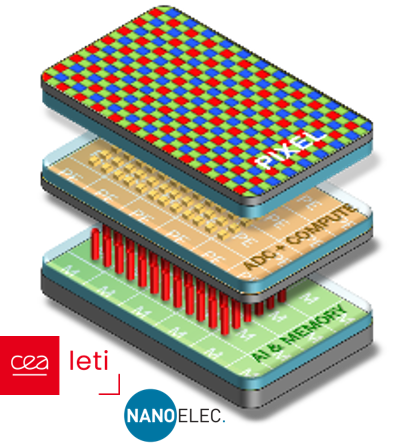
Figure 1: Illustration of a 3-layer smart imager where layer 1 is the pixel layer (photodiode),
layer 2 is the analog/digital signal processing layer, and layer 3 is the AI layer.
SOURCE: IRT Nanoelec
Development of 1x10μm highdensity TSVs
TSVs are essential for 3DICs as they enable dense vertical interconnections that reduce latency and increase bandwidth. As part of a 3-layer image sensor, they create the conditions for the integration of additional functionalities, such as AI for more advanced processing capabilitie s , directly within the sensor, thereby enhancing its overall performance and versatility. HD TSVs with a diameter of 1μm were first developed with a height of 10μm [2]. Indeed, due to the limited precision of the thinning process, a total thickness variation (TTV) of around 3μm could be achieved across wafers. Consequently, a silicon thickness of less than 9μm would have been irrelevant in view of the nonuniformity of the grinding step, and in these conditions, the electrical resistance scattering, caused by the more than 30% variation in total height, would have been unacceptable. The aspect ratio (AR) of these TSVs, at 10:1, was quite challenging in terms of process as plasma-enhanced chemical vapor deposition (PECVD) processes are barely capable of reaching the bottom of such high AR cavities. Consequently, a poor step coverage was expected for the dielectric liner meant to insulate the metal TSVs from the surrounding silicon. This limitation was revealed on a basic 1-layer (1L) test vehicle (TV). Using just one damascene level located on each side of a thin wafer oxideoxide bonded to a carrier, this 1L TV was used to characterize the HD TSVs, independently of the assembly (without contributions from hybrid bonding pads or vias) (Figure 2).
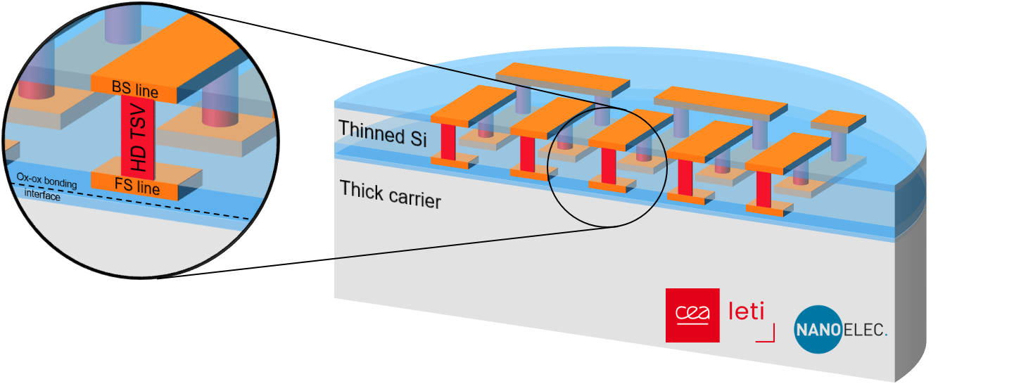
Figure 2: Schematic representation of the “1L” test vehicle used to characterize the HD TSVs.
SOURCE: CEA-Leti/J. Charbonnier
Characterization included the implementation of daisy chain structures with a pitch of 2μm (Figure 3a), which produced a conduction yield of 100% over 10,000 HD TSVs, demonstrating that connections to both good. We then used Kelvin structures with one isolated TSV (Figure 3b) to accurately measure the electrical resistance of a single TSV without contributions from the feeding lines. A median value of less than 1Ω, with a minimum value of around 500mΩ, was obtained. However, on specif ic Kelvin structures with a dense matrix of HD TSVs (2μm pitch) around the device under test (DUT), the resistance measurement was per turbed, most l ikely due to leakage between the dummy TSVs. Therefore, some of the current f lowing from the top line to the bot tom line probably transited through dummy TSVs instead of or in addition to flowing through the DUT. Morphological characterizations by scanning electron microscope (SEM) confirmed that contact with the top and bottom lines was good, and that there was an absence of voids inside the copper cylinders. The overlay between the TSVs and the landing pads (front-side line) was remarkably good (<50nm). More generally, a |Mean|+3σ of just 65nm was measured across entire wafers, obtained thanks to a field-byfield alignment that compensated the map distortion due to the bonding. Additional cross-sectional micrographs also confirmed that the insulation liner was insufficiently thick, with a high probability of discontinuities along the sidewalls because of the limitations of the PECVD deposit ion process. Nevertheless, we implemented the same TSVs in more complex TVs to test their connectivity in multi-layer architectures involving hybrid bonding. The next sections discuss TV development.
Figure 3: Layout top-views and cross-sectional SEM micrographs of 1x10μm HD TSVs in a 1L architecture:
a) dense environment (2μm pitch daisychain);
and b) isolated area (Kelvin structure.
Demonstration of 2-layer and 3-layer integrations
We have designed a 3-layer (3L) TV that incorporates two Cu-Cu hybrid bonding interfaces, face-to-face (F2F) and face-to-back (F2B), with one layer containing 1x10μm HD TSVs. The 3L TV is composed of three 300mm wafers, each formed from three stacked damascene levels: a metal line level (MZ), a hybrid bonding via (HBV) level, and a hybrid bonding metal (HBM) level. After F2F hybrid bonding of the first two wafers, the silicon of the upper wafer is thinned to 10μm to allow fabrication of the TSVs within the remaining thin silicon layer. Once the bonding pads have been added on top of the TSVs, F2B hybrid bonding can be per formed before removing the si l icon of the upper wafer. Lastly, following deposition and opening of the passivation layer, the final copper pads are patterned. For this type of 3D integration, the main challenge is to integrate TSV interconnects within a hybrid bonding f low to allow F2B hybr id bonding after TSV fabrication. To demonstrate the feasibility of the integration, we f i rst developed a 2-layer (2L) TV. In this context, controlled chemical mechanical polishing (CMP) is the key process making it possible to obtain a f lat surface with very low nanotopography and roughness after TSV integration. In
Figure 4, we show a SEM crosssection image of our 2L TV. Good electrical connectivity was obtained, as demonstrated by electrical tests of Kelvin and daisy chain structures, with a total resistance close to 1Ω using 1x10μm HD TSVs [3]. Having demonstrated the feasibility of integrating HD TSVs compatible with a F2B hybrid bonding step, we worked on the 3L TV manufacturing process , with three wafer and two hybrid bonding steps, and characterized the resulting device [4].
Figure 4: FIB-SEM cross-section of the 2L TV: the pitch is 6μm for the bonding pads; and the HD TSVs’ dimensions are 1x10μm.
SOURCE: CEA-Leti
As part of the characterization, we developed a focused ion beam (FIB)- SEM 3D cross-section technique to image two perpendicular cross sections at the same location, making it possible to simultaneously view the structure in both X and Y directions (Figure 5). The 3D cross section reveals good connectivity between the damascene layers, including TSVs. In addition to these morphological characterizations, we performed electrical tests on Kelvin and daisy chain structures to demonstrate the functionality of our 3L TV.
Figure 5: FIB-SEM 3D cross-section of the 3L TV structure: the pitch is 6μm for the bonding pads; and the HD TSVs’ dimensions are 1x10μm. SOURCE: CEA-Leti/L. Sanchez
On daisy chain structures, with a half-link number between 12 and 6,480 (Figure 6), we obtained a median resistance around 2 . 5Ω per unit with ver y low dispersion for the core population (80% of the total population). These results are very satisfactory. Nevertheless , we are continuing to improve the manufacturing process to reduce the resistance of the structure as much as possible. It is also now possible to change the configuration of the 3L TV structure by using shorter TSV interconnect ions, to manufacture 1x6μm TSVs instead of 1x10μm TSVs. These shor ter structures reduce the resistance of the 3L structure.
Figure 6: Transmission electron microscopy (TEM) cross section of the 2-CMOS layer stacking including
Daisy chain half-link cumulative percentage resistance for the 3L TV with a 6μm pitch and 1x10μm HD TSVs. SOURCE: CEA-Leti
Developing 1x6μm HD TSVs and implementation in a 2L TV
To overcome the leakage is sue between TSVs, we reduced their AR. To retain the same density, we did not increase their diameter, rather we decreased their height. To do so, we first improved the thinning process, reducing the TTV to 1μm. With a dispersion of ±10%, it became possible to consider thinning the silicon to 5μm. Consequently, we switched to a TSV geometry of 1x6μm (including top and bottom oxide layers) instead of the original 1x10μm. This reduction in AR improved the step coverage of the insulation liner and solved the leakage issue. Shortening the TSVs by 40% reduced their electrical resistance proportionately [5]. After electrically and morphologically character izing the 1x6μm HD TSVs in a 1L TV (Figure 7), we successfully implemented them in a 2L TV.
Figure 7: Cross-sectional SEM micrographs of 1x6μm HD TSVs in a 1L architecture: a) overall view in a dense area (2μm pitch);
b) a zoomed-in view at the top of the HD TSVs; and c) a zoomed-in view at the base of the HD TSVs.
iBEOL with Cu/ULK 28nm.
SOURCE: CEA-Leti
The connection yield on daisy chains remained close to 100%, validating the compatibility of our 1x6μm HD TSVs with the constraints of hybr id bonding. The electrical resist ance measured on a Kelvin st ructure (including contributions from HB pads and vias) was in line with our expectations, with a median value of 1.2Ω. Finally, SEM confirmed that the morphology of the TSVs and the hybrid bonding interfaces were compliant (Figure 8). This validation on a 2L architecture bodes well for implementation in 3L TVs (in progress) and functional smart imagers.
Figure 8: Cross-sectional SEM micrographs of 1x6μm HD TSVs in a 2L architecture: a) overall view in a dense area (4μm pitch);
b) a zoomed-in view at the base of the HD TSVs; and c) a zoomed-in view at the top of the HD TSVs.
SOURCE: CEA-Leti
On the path to 3-layer smart imagers manufacturing
The technologies and results reported
here by CEA-Leti and its IRT Smart
Imager Program partners are key steps
in the development of future generations
of smart imagers. The reduction of the
pixel size will continue, as will attempts
to improve performance and add new
functionalities. By providing high-density
and low-resistance interconnects, hybrid
bonding combined with HD-TSVs will
significantly contribute to future progress.
The reduction of hybrid bonding pitch is
currently mainly driven by memories and
chiplets, but it remains a key technology
for imaging sensors. HD-TSVs also play
a crucial role in 3D interconnection
providing a pathway for efficient signal
transfer and power distribution between
vertically-stacked layers.
CEA-Leti’s recent demonst ration
of 1x6μm HD TSVs showed excellent
morphological and electrical results,
achieved thanks to an improved thinning
process, reducing the TTV to 1μm.
The shorter TSVs length reduced the
electrical resistance as well as the AR,
creating the conditions for improved
oxide liner deposition and thereby,
enhanced electrical insulation. CEA-Leti
has optimized the processes to make HD
TSVs compatible with hybrid bonding—
therefore, F2B hybrid bonding can be
performed after HD TSVs fabrication.
The manufacture and testing of a 3-layer
demonstrator proves the feasibility of
3-layer architecture combining fine-pitch
HD TSVs with hybrid bonding in faceto-
face and face-to-back configurations,
and paves the way for the manufacture of
3-layer smart imagers.
In parallel to these technological
developments, IRT Nanoelec partners
are tackling the challenges related to
3D design tools and computer-aided
design (CAD) flow (analog and mixedsignal
simulation, high-level synthesis,
place and route, thermal, design for
test, and process design kits [PDKITs]).
Opt imized architectures are being
defined, and partitioning solutions, as
well as neural network optimization, are
being studied. All these developments
will contribute to the next generation of
smart imagers offering AI functionalities.
The partners involved in the IRT Smart
Imager Program are already working on
the demonstration of functional 3-layer
smart imagers.
Summary
This article focuses on the silicon technology developments done by CEALeti regarding wafer-to-wafer hybrid bonding and HD TSVs and it presents the recent demonstrations of 2-layer and 3-layer stacking integrations. These demonstrations, together with the work done by other partners of the IRT Smart Imager Program (STMicroelectronics, Siemens EDA, Prophesee, Lynred, Grenoble INP-UGA) on applications and architecture studies, design tools and methodologies, and neural networks optimizations, are key and pave the way for the next generation of smart imagers.
Acknowledgment
This work was suppor ted by the French National Research Agency (ANR) through the “Investissement d’avenir” (investments for the future) programs: ANR 10-AIRT-0005 (IRT NANO-ELEC).
About Stéphan Borel
Stéphan Borel is Project Leader at CEA-Leti, Grenoble, France. He joined Leti in 2001; after 6 years as a process engineer and 4 years in process integration, he moved to Leti’s packaging lab to manage various technological projects involving 3D integration. His current focus is interconnections, specifically TSVs for next-generation components, including smart imagers. He has an Engineering degree from Grenoble Institute of Technology, France.
About Stéphane Nicolas
Stéphane Nicolas is Project Leader at CEA-Leti, Grenoble, France. He worked for 10 years in the industry (Corning and Tronics/TDK) developing new integration packaging technologies for MEMS products before joining CEA-Leti in 2009, where he has continued to work on 3D integration solutions for MEMS packaging. He has also been involved in the development of new 3D technologies involving Cu-Cu hybrid bonding and high-density TSV for CMOS image sensor applications. He received a PhD in Microtechnology at Pierre et Marie Curie U.